Welcome to my web page dedicated to active electronic components
On this page I will try to define with words suitable for everyone the immense world behind the simple phrase "active electronic components", it is not an easy task but I will try. Of course, as already mentioned on the other pages, it is impossible to condense a very vast subject in this small text, but if you intend to deepen or need professional advice, you can contact me via the Contacts page.
At this link you can find the page dedicated to electrical engineering and electronics, while at this link you will find the page dedicated to passive electronic components.
The electronics active components
While the passive components have had a dimensional and qualitative evolution only, on the contrary the active components have experienced real earthquakes in their evolution over time, with entire systems and production concepts disappeared, replaced by other revolutionary production systems and concepts, we moved from thermionic (or vacuum) components to solid state systems around 1960, which started the revolution that allowed us to create everything we see now (smartphones, liquid crystal TVs, personal computers, tablets).
Now let's get to know the main active components, they are transformers, thermionic tubes (also called valves), transistors and integrated circuits.
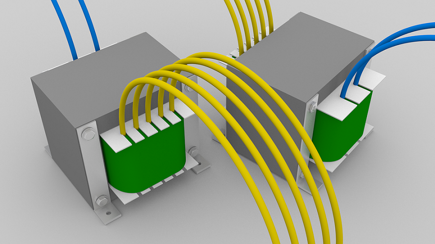
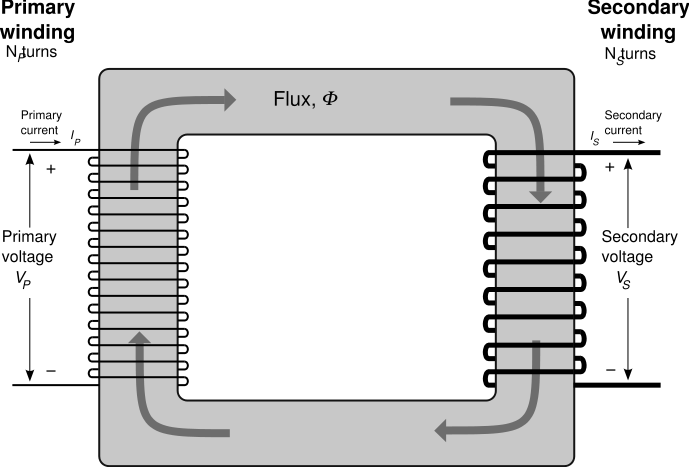
The transformers are defined "active machines without moving parts" they are formed by two coils of copper wires mounted on a pack of laminations and separated by a core (see images at the end of the discussion), the coils are called a "primary" and the other "secondary" depending on the direction of operation. The transformers allow through the law of electromagnetic induction (Faraday-Neumann-Lenz law) to transfer by lowering or raising the value (transformation ratio), voltages and electric currents, they also ensure the physical separation between circuits, since between primary and secondary there is no contact, and they also act as impedance adapters in professional audio equipment. The size of a transformer depends on the current and the voltage it has to manage, the working voltage and current values are usually printed directly on the transformer itself.
![]()

Low voltage transformers with various secondary (yellow wires) Transformer electrical symbol
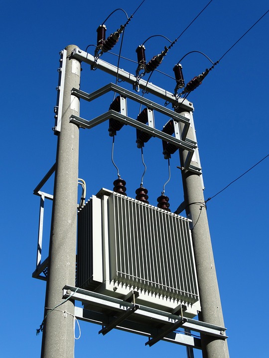
Three-phase high voltage transformer mounted on poles. Principle of operation
Vacuum active components
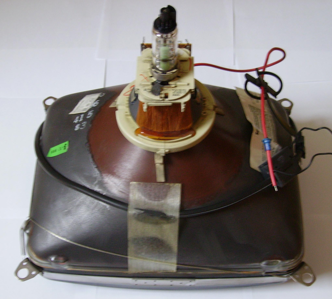
The thermoionic tubes or electronic tubes were the first active components to allow the amplification and processing of electronic signals, TVs, radios, transmitters, and even computers (of gigantic size) were made with them. They exploit the thermionic emission, which consists in the emission of electrons in the vacuum, by an electrode called "cathode", negatively polarized, made of a particular material, which is heated by an incandescent tungsten filament, the electrons emitted by moving in the vacuum they have no particular obstacle and are attracted and collected by another positively polarized electrode called an anode or plate, this is the thermionic diode, a component (available in the solid state version as a silicon diode) that is passed through by the current in one direction only (direct bias) and not in the other (reverse bias).
If we add a third electrode
called a grid between anode and cathode, and we
polarize it in a slightly negative way, we will be able to control and
modulate the flow of electrons moving in the vacuum, in other words by
applying a small signal to the grid we will obtain a very wider on the
anode, we have thus created a
triode, the simplest thermoionic device, and also the first one
capable of amplifying an electrical signal, the electrodes are enclosed
in a glass bulb in which the vacuum has been obtained. If you need
further information, you can go to the
contact section.
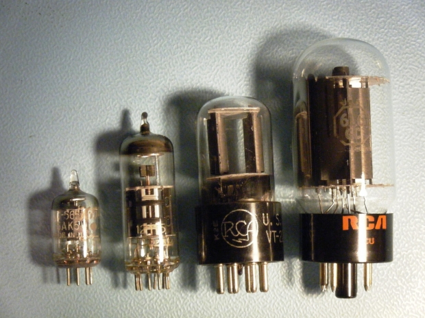
Multigrid tubes were manufactured to meet
particular needs, tetrodes (two grids), pentodes (three
grids) and tubes having in the ampulla not a vacuum but a rarefied gas.
Although replaced in almost all applications by
solid-state devices, they continue to be irreplaceable in some
equipment, such as
high-frequency high-power amplifiers and high-end hi-fi applications
for the particular mellow and pure sound that they manage to achieve.
produce, even in the microwave oven that we all have at home there is a
high-power valve that produces the very short-term emissions that cook
food. And the cathode ray tube that until a few years ago allowed you to
see splendid images on CRT TVs was a
valve with the screen acting as an anode.
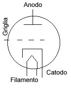
Thermoionic tubes for radio and hi-fi applications Electrical symbol of the vacuum triode
Principle of operation of the triode
Solid state electronic devices
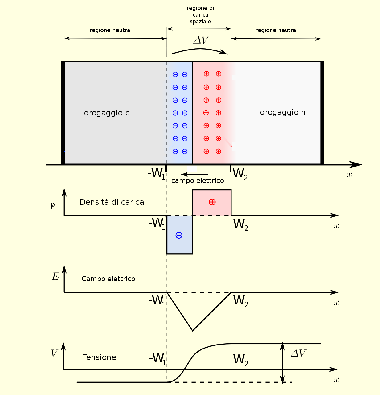
They are particular active electronic components built by doping (introducing impurities) suitably a semiconductor material (germanium, silicon or artificial semiconductors), the semiconductors are doped with positively charged P type impurities (hole or lack of electron) or negatively charged N type (excess of electrons), the contact between a P-charged semiconductor with another N-charged semiconductor produces a PN-type junction, in the contact area a current called depletion is created due to the exchange of charges in an attempt to restore the neutrality of the materials, thus creating a neutral zone near the contact and a small insulating layer at the contact itself. It should be noted that the PN junction subjected to direct sunlight is able to produce an electrical voltage of 0.6V in the contact area, therefore it becomes a solar cell with a photovoltaic effect, by arranging many junctions (series and parallel) in an appropriate way. they get the photovoltaic panels currently used in production plants. If you need further information you can go to the contact page or you can go to this link.
Using the properties of the PN junction it is possible to obtain all the components that are the basis of modern electronics, including solid state diodes, TRANSISTOR, MOSFET, JFET, UJT, these components can be made both in discrete form, i.e. as a single component with certain characteristics, or as an integrated circuit, or a semiconductor crystal that doped in an appropriate way, allows to obtain a complete circuit of passive and active components in very little space and with great savings in material and time, but let's get to know more from near the various types of semiconductor components. Click on the images to enlarge them
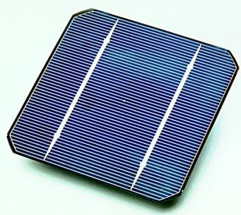
Graphic illustration of P-N junction Photovoltaic cell obtained by means of a suitable connection of P-N junctions
The semiconductor diode uses a single P-N junction, due to its known properties, it is able to be crossed by current or not depending on how we apply voltage to it. It has two external connections, one leads to the doped semiconductor P (anode), the other to the N one (cathode), if we apply the voltage with the positive pole to the anode and the negative one to the cathode, the diode will be passed through by the current (direct bias), if instead we invert the poles the current will not be able to cross the diode (reverse bias), they are used as rectifiers in power supplies, as switches, as detectors and as protection (combined with a fuse) from reverse polarity of the ' supply.
It should be borne in mind that the diodes have a threshold voltage of 0.6V for silicon ones and 0.2V for germanium ones, i.e. if the voltage across them does not exceed this value they behave like an open switch (no current flows ), silicon diodes with a lower threshold (Schottky diode) are manufactured, diodes that are used as variable capacitors (varicap diode) by varying the voltage across them and particular voltage stabilizing diodes called Zener diodes. Impossible not to mention the L.E.D. (light emitter diode), particular diodes that emit light from the PN junction, then amplified by a special lens, they are revolutionizing the lighting sector thanks to the very low current consumption and the particular light they can produce, from simple indicators they are they have evolved with the increase in the light emitted and with the achievement of white light, lamps of all types and colors are currently manufactured, and also provide backlighting for the LCD (edge LED) screens of the latest generation TVs.
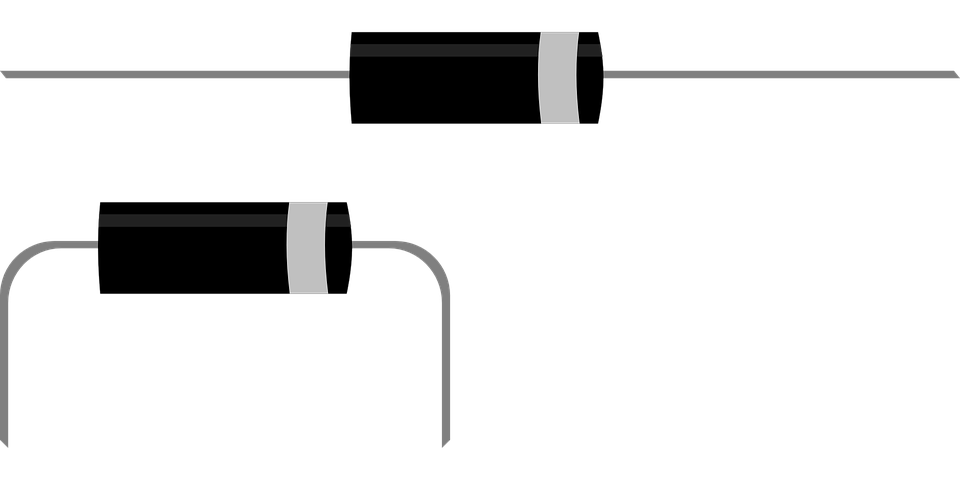

Real diode, the white band is the cathode Symbol of the diode used in the wiring diagrams
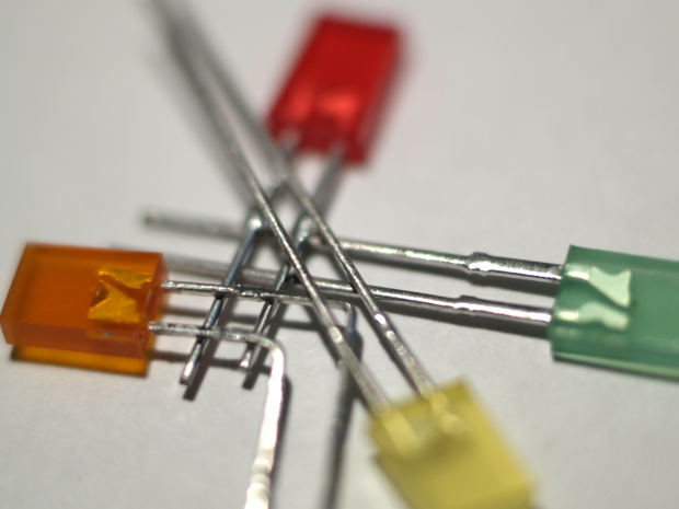
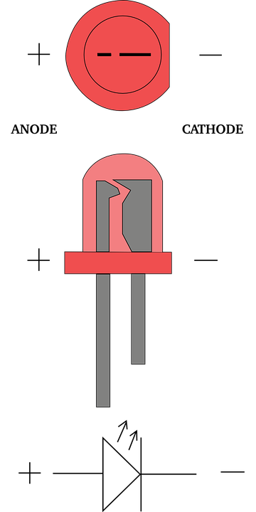
LEDs of various colors Internal diagram and symbol of the LED diode
If you need further information or professional advice, you can go to the contact page.
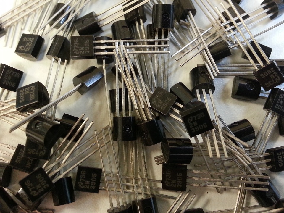
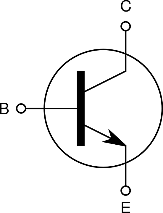
The classic bipolar transistor or BJT (bipolar junction transistor) is a component formed by two PN junctions (see figure below), it can be of the PNP type operating with a positive current (electron holes) or of the NPN type operating a current type negative (electrons), and has three terminals called, Base, Collector, Emitter (indicated in the electrical symbol by an arrow). It was discovered in 1946 in the Bell telephone labs by researchers Walter Brattain, John Bardeen and William Schockley, they gave birth to modern electronics.
The transistor is an active component capable of amplifying the signals applied to it, such as the thermionic triode, but with many advantages, the main ones are that of being a solid state therefore difficult to destroy mechanically, it is small in size if compared to the tubes, it works with low voltages at the ends and its integration is relatively easy, moreover it does not require filament tension. Very schematically, its operation can be defined in this way, "the electrons emitted by the emitter are regulated by the base and then collected by the collector", in practice the emitter current Ie is regulated as a tap does with water from the current of base Ib, finally on the collector we find the regulated and amplified current Ic.
The transistor to work correctly must be polarized in the right way according to the type of operation required, to do so using passive electronic components such as resistors and capacitors.
TheTransistors are used as amplifiers, switches, oscillators, regulators (combined with a Zener diode) and many other applications. As the solid state component technique progressed, other transistors optimized for some applications were introduced, including the JFET junction field effect transistor, the metal MOSFET -oxide-semiconductor field-effect transistor (voltage command, high input impedance, switch with low channel resistance when directly biased) and the UJT or unijunction (pulse oscillator).
The transistors are enclosed in metal or plastic containers depending on the required power dissipation and the possible application of a heat sink.
![]()
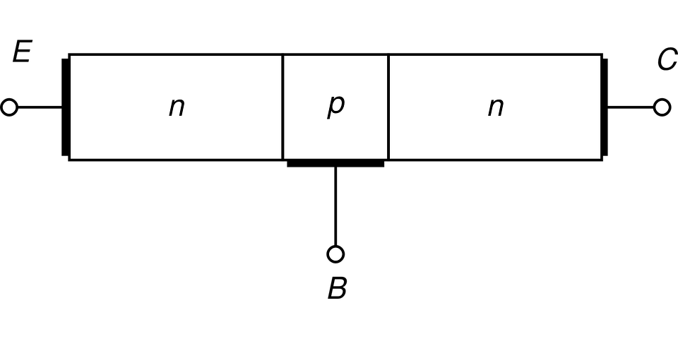
BJT NPN transistor obtained from a semiconductor bar Symbol of the BJT NPN transistor (PNP is represented with an inverted arrow)
![]()
![]()
Power transistor with TO220 package Small signal transistor in TO92 package
![]()
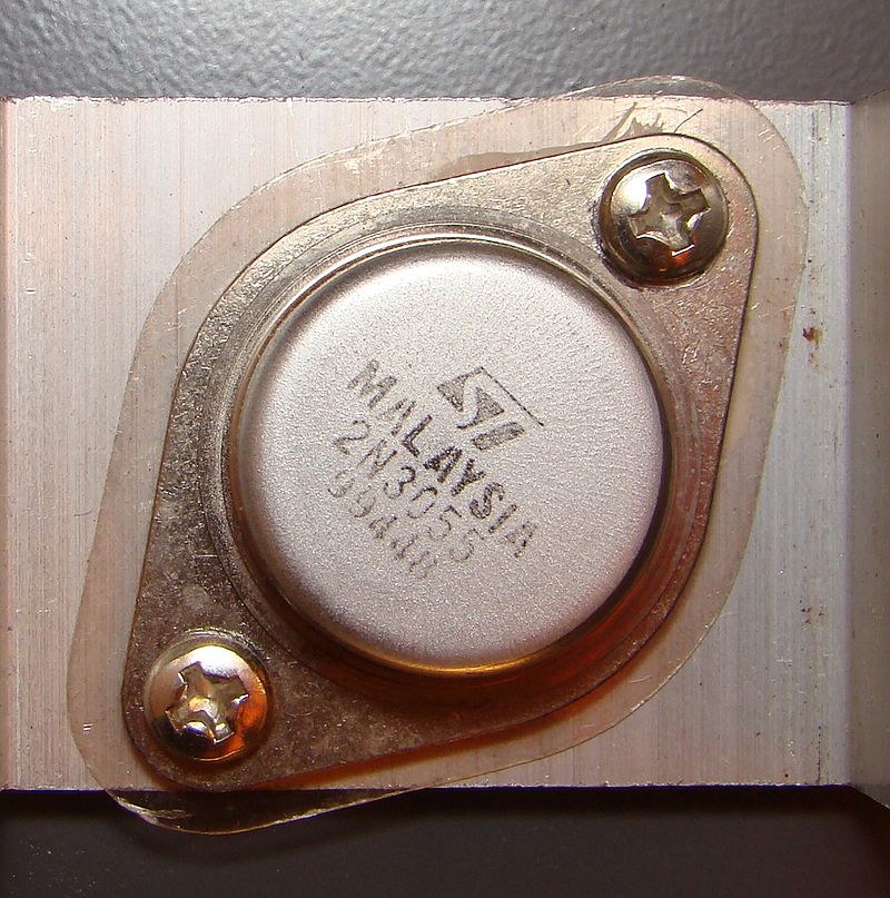
Small signal transistor in TO18 package 2N3055 metal power transistor in TO3 package
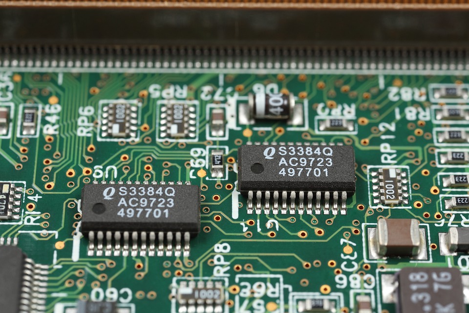
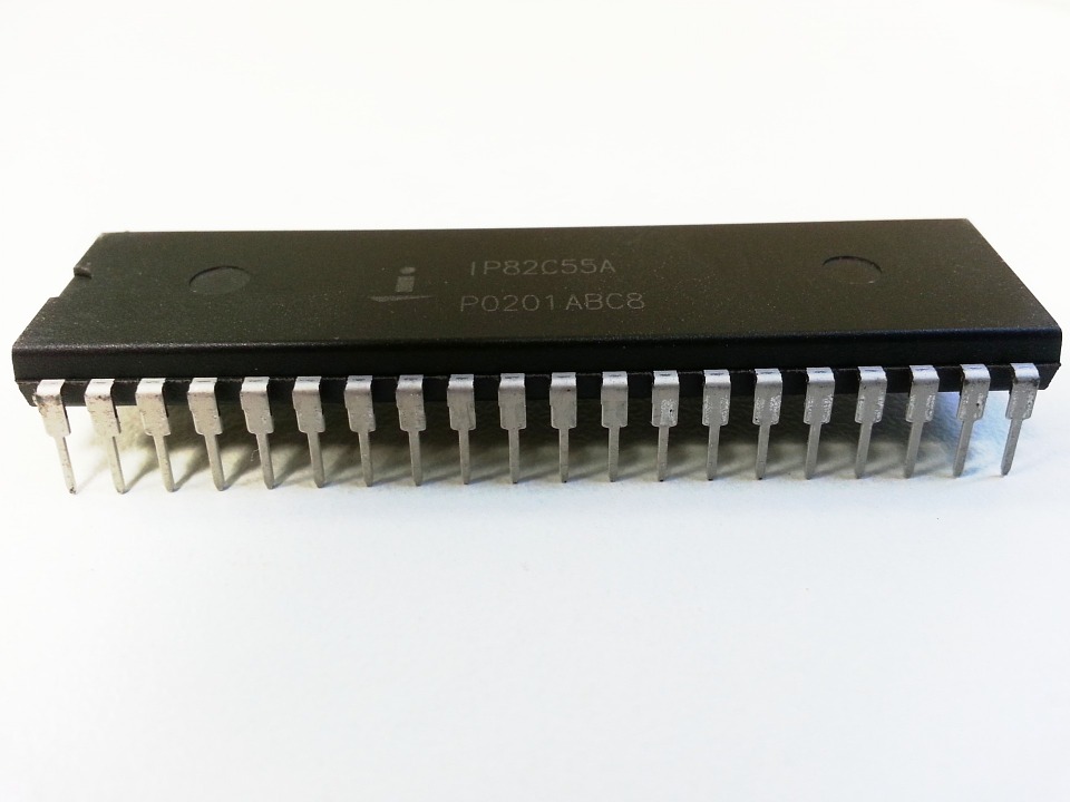
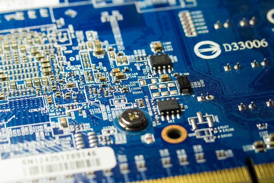
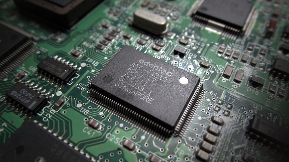
Finally, monolithic integrated circuits are made by doping the areas of a semiconductor chip in a suitable way, in detail, by introducing more or less conductive impurities, insulators or conductors (or resistors of the desired value) will be created, impurities of type P or N will create transistors with the desired characteristics, by doing so a complex circuit will be obtained on a small semiconductor chip, accessible from the outside with terminals so as to be able to connect to the outside the components necessary for operation but not integrable (inductances, capacitors, resistors and more ).
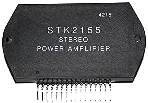
There are analog and digital integrated circuits that perform very complex functions, it is thanks to them that electronic circuits have been miniaturized, with results visible to all, just think of tablets or smartphones, real miracles of electronic technology. Integrated circuits are also produced built with normal components, without a container, then enclosed in plastic containers and performing however simple functions, these types of components are called "hybrid integrated circuits". The hybrid amplifiers of the STK series are a very common example.
To know the characteristics of the active components, you must have the relevant datasheets. The datasheets are information sheets, issued by the manufacturer where you can find all the information about the maximum and minimum operating parameters of the components, and even examples of realizations, an excellent site where you can find datasheets of almost all the active components you can find at this link. Instead, by clicking with the mouse on this link you can view the easy-to-understand datasheet of a well-known component that has been in the breach for many years, the strange low frequency amplifier TDA2003, capable of producing about ten Watts, using few external components, you will also find it in the datasheet. internal schematic of the component, and construction examples.
Dual in line digital integrated circuit Dual in line SMD integrated circuit
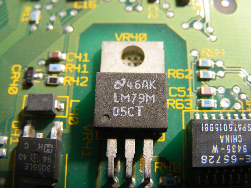
Integrated cicuit voltage regulator 5V negative Integrated circuit digital flatpack SMD
Of course it is impossible to condense all these concepts in a small space, mine is just a good guide for those who are looking into this fantastic world, it is still possible to deepen or request professional advice by contacting me, for this go to the contact page.
Thank you for visiting my website and
following my guide, please come back and visit it.
Electrical engineering and electronics Passive components
Home
Informatics, Computer networks , Software and operative system
Electronics, Active components, Passive components
Radiotecnics
Seismology
Contacts
Who i am
Audio
Created and mantained by Armando Caligiuri (C) 2024 Version 3.2 ext
Armando Caligiuri, Electronic senior expert, Electronic and I.T. maintainer, electronic project implementer, I.T. consultant
Webmaster Armando Caligiuri, for the use of the contents of the site visit the Disclaimer page